FMS 2020 Keynotes & Sessions
Please note: Some Sessions are ONLY available to paid attendees marked (PRO).
Sessions marked (OPEN) are available to all.
Day 1 Intro Tue 8:35am
Introduction
to Day 1 of Virtual FMS
Jay Kramer
Network Storage
Jillian Coffin
TechTarget
FMS
Keynote 1 Tue 10:15am

Today's Trends in Cloud and the Future Enterprise (OPEN)
Matt Eastwood
Senior Vice President
IDC
Keynote 2 Tue 11:35am

MRAM Stars in an AI Coprocessor for NASA Spaceflight Computing (OPEN)
Jack Guedj
CEO
Numem
Keynote 3 Tue 1:15pm

Storage as the Driver of Change: Rethinking Data Infrastructure (OPEN)
Siva Sivaram
President of Technology
and Strategy
Western Digital
Keynote 4 Tue 1:55 pm
Using Hardware Acceleration to Increase NVMe Storage Performance (OPEN)
Thad Omura
VP Marketing Flash Business Unit
Marvell
Marvell Semiconductor
Keynote 5 Tue 4:15pm

Fungible Data Centers: The Evolution of Data Centers in the Data-Centric Era (OPEN)
Pradeep SIndhu
Co-Founder and CEO
Fungible
Keynote 6 Wed 10:15am

Bringing AI/ML to Data Centers Everywhere Via GPUs, DPUs, and Matching Storage (OPEN)
Kevin Deierling
VP Marketing
NVIDIA/Mellanox
Keynote 7 Wed 11:35am

The Future Adaptable Data Center (OPEN)
Gopi Jandhyala
VP of Datacenter Engineering
Xilinx
Keynote 8 Wed 1:15pm

Storage Processors to Unleash the Full Potential of Flash Storage (OPEN)
Steve Fingerhut
Presidents, CBO
Pliops
Keynote 9 Wed 1:45pm

Intel® Optane™ Persistent Memory: From Vision to Reality (OPEN)
Alper Ilkbahar
Vice President of Data Products Group
Intel
Keynote 10 Wed 3:55pm

Persistent Memory Meets the Data Needs of Demanding Applications (OPEN)
Alistair Symon
VP of Storage Development and Software Defined Environments
IBM Storage
Keynote 11 Wed 4:25pm

New Flash Architecture Combines QLC Density with SLC Speed (OPEN)
Andy Hsu
Founder and CEO
NEO Semiconductor
Keynote 12 Thu 10:25am

NVM Express Technology: Powering the Connected Universe
Amber Huffman
Intel Fellow and Chief Technologist
NVM Express
Keynote 13 Thu 11:45am

Accelerating Deep Neural Networks with Analog Nonvolatile Memory Devices (OPEN)
Geoffrey Burr
Distinguished Research Staff Member
IBM Almaden/AI
Keynote 14 Thu 12:15pm

What You Need to Know about DNA Data Storage Today (OPEN)
Karin Strauss
Title to Come
Microsoft
Session A-1 Tue 8:35am
What The Hyperscalers Are Buying (PRO)
Jonathan Hinkle
Executive Director
Lenovo
Session B-1 Tue 8:35am
NVMe-oF: The Best Way to Network Enterprise Storage (OPEN)
John Kim
Director of Storage Marketing
NVIDIA
Session C-1 Tue 8:35am
Advances in Enterprise Flash Storage (OPEN)
Jay Kramer
Business Chairperson and Emcee
Network Storage
Session D-1 Tue 8:35am
Smart New Architecture for Cloud-Scale Storage (OPEN)
Shachar Fienblit
VP R&D/Co-Founder
VAST Data
Session A-2 Tue 10:45am
Hyperscale Storage in 2025 and How We Got There (Panel) (PRO)
Jonathan Hinkle
Executive Director
Lenovo
Session B-2 Tue 10:45am
NVMe/TCP Use Cases (Panel) (OPEN)
Howard Marks
Technologist Extraordinary
VAST Data
Session C-2 Tue 10:15am
Top Ten Things You Need to Know about Enterprise Storage Today (Panel) (OPEN)
Jean S. Bozman
President
Cloud Architects
Session D-2 Tue 10:45am
Using Cloud-Defined Storage (Panel) OPEN
J Metz
Board Member
SNIA
Pres.1 Tue 11:25am
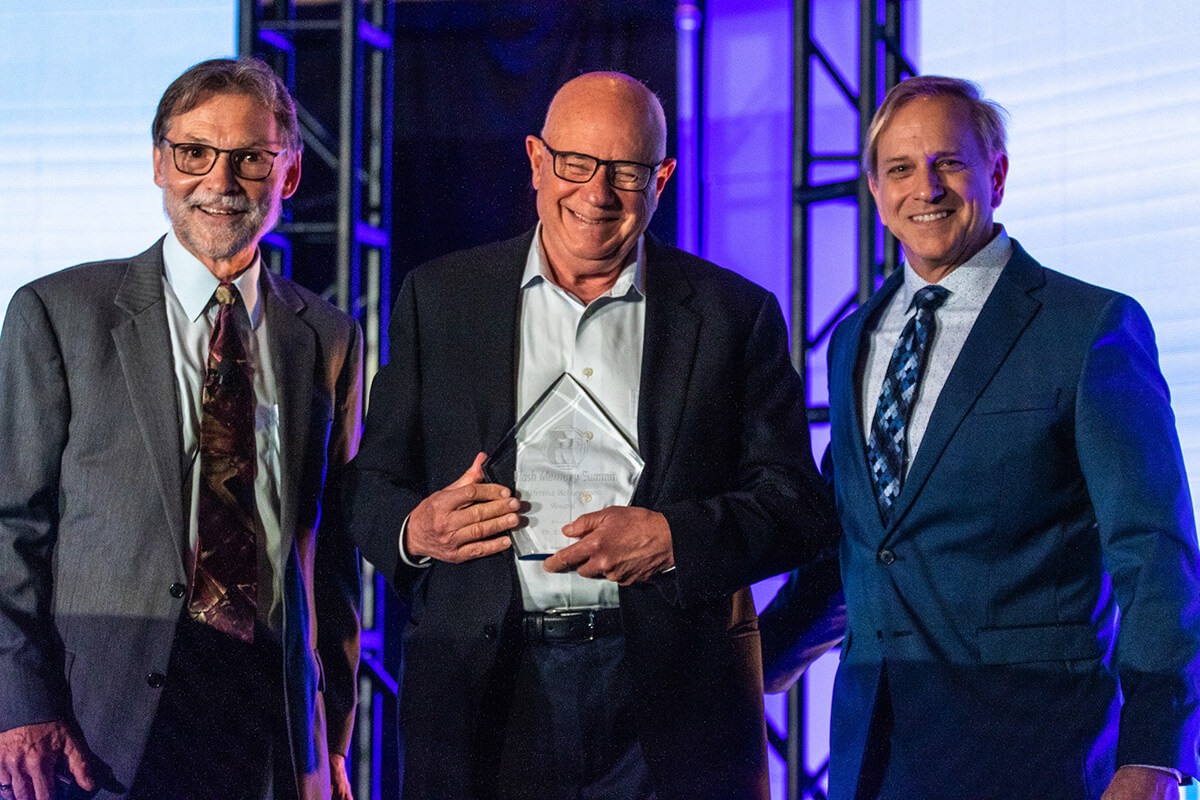
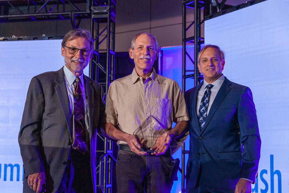
Lifetime Achievement Award (OPEN)
Chuck Sobey
Founder
Channel Science
Pres.2 Tue 1:05pm
TechTarget (OPEN)
Jillian Coffin
Group Publisher Storage, Virtualization & Cloud Media Groups
TechTarget
Pres.3 Tue 1:45pm
SNIA (OPEN)
Willie Nelson
CMSI Marketing Chair
SNIA
Session A-3 Tue 2:35pm
Using 3D XPoint to Overcome Storage Roadblocks (PRO)
Milind Weling
Sr. VP Programs and Operations
Intermolecular
Session B-3 Tue 2:35pm
Getting the Most Out of NVMe (OPEN) (Sponsored by NVM Express)
Cameron Brett
Director of Enterprise SSD Marketing
KIOXIA
Session C-3 Tue 2:35pm
How Data Centers Can Profit from New Memory Technologies (OPEN)
Dave Eggleston
Owner and Principal
Intuitive Cognition
Session D-3 Tue 2:35pm
Bringing Enterprise-Class Management to Big Memory (OPEN)
Frank Berry
VP Marketing
MemVerge
Session A-4 Tue 4:45pm
3D XPoint in 2025, and How We Got There (Panel) (PRO)
Mark Webb
Principal/Consultant
MKW Ventures
Session B-4 Tue 4:45pm
NVMe in Cloud Applications (Panel) (OPEN)
Mark Carlson
Principal Engineer Industry Standards
KIOXIA
Session C-4 Tue 4:45pm
What Will Replace Flash and When? (Panel) (OPEN)
Jim Handy
President
Objective Analysis
Session D-4 Tue 4:45pm
Top Ten Things You Need to Know about Big Memory Management Today (Panel) (OPEN)
Chuck Sobey
Founder
Channel Science
Day 2 Intro Wed 8:30am
Introduction
to Day 2 of Virtual FMS
Jay Kramer
Network Storage
Jillian Coffin
TechTarget
FMS
Session A-5 Wed 8:35am
Accelerating Applications for a Competitive Edge (PRO) (Sponsored by Micron)
Brian Berg
President
Berg Software Design
Session B-5 Wed 8:35am
Persistent Memory (PM) Offers Storage at Memory Speeds (OPEN) (Sponsored by JEDEC, SNIA, and OpenFabrics Alliance)
Jim Pappas
Director of Technology Initiatives
Intel Corporation
Session C-5 Wed 8:35am
IDC Enterprise/Cloud Storage - Part 1 (OPEN)
Eric Burgener
Research VP, Infrastructure Systems and Platforms
IDC
Session D-5 Wed 8:35xx
Storage Processors Accelerate Database Operations (OPEN)
Tony Afshary
Sr. Director of Product Marketing
Pliops
Session A-6 Wed 10:45am
Which Type of SSD Is Best for Your Application? (Panel) (PRO)
Brian Berg
President
Berg Software Design
Session B-6 Wed 10:45am
How Can We Solve the Problems Holding Up Persistent Memory Adoption? (Panel) (OPEN) (Sponsored by JEDEC, SNIA, and OpenFabrics Alliance)
Dave Eggleston
Owner and Principal
Intuitive Cognition
Session C-6 Wed 10:45am
IDC Cloud Storage - Part 2 (OPEN)
Eric Burgener
Research VP, Infrastructure Systems and Platforms
IDC
Session D-6 Wed 10:45am
Optimizing NVMe-oF Storage with EBOFs & Open Source Software (OPEN) (Sponsored by Micron)
Sujit Somandepalli
Principal Storage Solutions Engineer
MIcron
Pres.4 Wed 11:25am
SuperWomen in Flash Leadership Award (OPEN)
Camberley Bates
Managing Director/Analyst
Evaluator Group
Pres.5 Wed 1:05pm
Virtual FMS Best of Show Awards (OPEN)
Business Chairperson and Emcee
Network Storage
Session A-7 Wed 2:15pm
New High-Speed Interfaces for Persistent Memory and Coprocessors (PRO)
Glenn Ward
Chief of Staff, Cloud Server Infrastructure
Microsoft
Session B-7 Wed 2:15pm
Ethernet-Attached SSDs Lead to Higher-Performing Storage (OPEN)
Rob Davis
VP of Storage
NVIDIA
Session C-7 Wed 2:15pm
IDC Enterprise Solid State Storage – Strategies and Futures (OPEN)
Eric Burgener
Research VP, Infrastructure Systems and Platforms
IDC
Session D-7 Wed 2:15pm
New Ways to Improve SSD Management and Performance (OPEN)
Jonmichael Hands
Senior Strategic Planner and NVM Express Marketing Work Group Chair
Intel Corporation
Session A-8 Wed 4:55pm
Where the New High-Speed Interfaces Fit and How They Work Together (Panel) (PRO)
Kurtis Bowman
President
Gen-Z Consortium
Session B-8 Wed 4:55pm
Top Five Ways Ethernet SSDs Can Improve Storage Solutions (Panel) (OPEN)
Rob Davis
Vice-President
NVIDIA
Session C-8 Wed 4:55pm
IDC Real World Applications and Solutions for Persistent Memory (Panel) (OPEN)
Eric Burgener
Research VP, IDC
TechTarget
Session D-8 Wed 4:55pm
Using the New EDSFF (E3) SSDs Effectively (Panel) (OPEN)
Cameron Brett
Director of Enterprise SSD Marketing
KIOXIA
Day 3 Intro Thu 8:30am
Introduction
to Day 3 of Virtual FMS
Jay Kramer
Network Storage
Jillian Coffin
TechTarget
FMS
Session A-9 Thu 8:35am
Computational Storage Increases System Throughput and Scalability (PRO) (Sponsored by SNIA)
J B Baker
Senior Director of Product Management
ScaleFlux
Session B-9 Thu 8:35am
Latest Trends in Storage for AI/ML (OPEN)
Sanhita Sarkar
Global Director, Analytics
Western Digital Corporation
Session C-9 Thu 8:35am
Flash Technology Advances Lead to New Storage Capabilities (OPEN)
Jung Yoon
Sr. Technical Staff Member
IBM
Session D-9 Thu 8:35am
Hands-on Testing of Persistent Memory’s Effects on Analytics Performance (OPEN)
Dennis Martin
Sr. Analyst
Principled Technologies
Pres.6 Thu 10:15am
IT Brand Pulse Awards (OPEN)
Frank Berry
VP Marketing
MemVerge
Session A-10 Thu 10:55am
Keys to Making Computational Storage Work in Your Applications (Panel) (PRO)
Jason Molgaard
Principal Storage Solutions Architect
Arm
Session B-10 Thu 10:55am
Storage for AI in 2025 and How We Got There (Panel) (OPEN)
J Metz
Board Member
SNIA
Session C-10 Thu 10:55am
Next Great Breakthrough in Flash Memory (Panel) (OPEN)
Leah Schoeb
Sr. Developer Relations Manager
AMD
Session D-10 Thu 10:55am
SmartNICs: The Key to High-Speed Converged Networks (Panel) (OPEN)
Rob Davis
Title DTB
NVIDIA
Pres.7 Thu 11:35am
UC Santa Cruz School of Engineering
Speaker TBD
Title TBD
UC Santa Cruz
Session A-11 Thu 1:45pm
Flash Controllers for Application Acceleration (PRO)
Erich Haratsch
Director of Engineering
Seagate
Session B-11 Thu 1:45pm
Storage for Model Training and Execution (OPEN)
Nisha Talagala
CEO and Founder
Pyxeda AI
Session C-11 Thu 1:45pm
SuperWomen in Flash (OPEN)
Camberley Bates
Managing Director/Analyst
Evaluator Group
Session D-11 Thu 1:45pm
Scaling of New Memory Technologies Used for Persistent Memory (OPEN
Mahendra Pakala
Managing Director Memory Group
Applied Materials
Session A-12 Thu 3:30pm
Multiprotocol NVMe Systems Offer Flexibility and Performance (Sponsored by Pavilion Data)
Keith Parker
Director of Product Marketing
Pavilion Data
Session B-12 Thu 3:30pm
Best Ways to Achieve AI Model Scalability (Panel) (OPEN)
Howard Marks
Technologist Extraordinary
VAST Data
Session C-12 Thu 3:30pm
Getting Serious about Containers and Flash Memory (Panel) (OPEN)
Jean S. Bozman
President
Cloud Architects
Session D-12 Thu 3:30pm
Will QLC SSDs Replace Hard Drives (Panel) (OPEN)
Randy Kerns
Senior Strategist
Evaluator Group
FMS 2020 Sponsors & Exhibitors
TechTarget-FMS 2020 Keynotes & Sessions
SearchStorage.com FMS 2020 Archives


